PCB INSPECTION
Snap a photo of any board and get six common defect types detected, boxed, and reported within seconds — built for quality inspection workstations and rework stations.
DEFECT COVERAGE
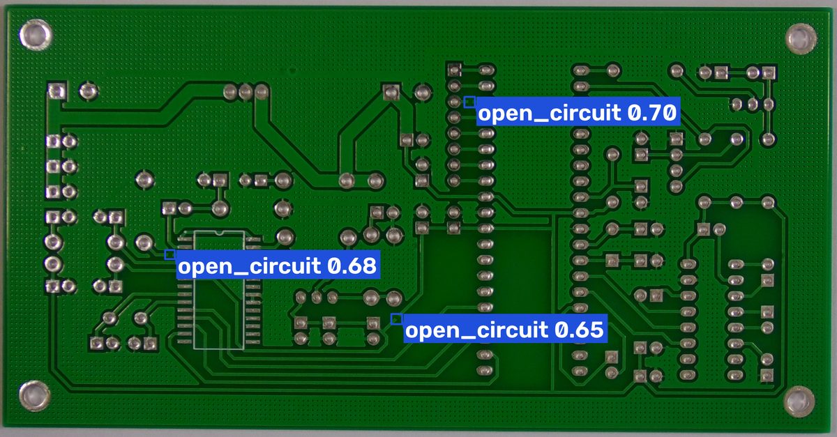
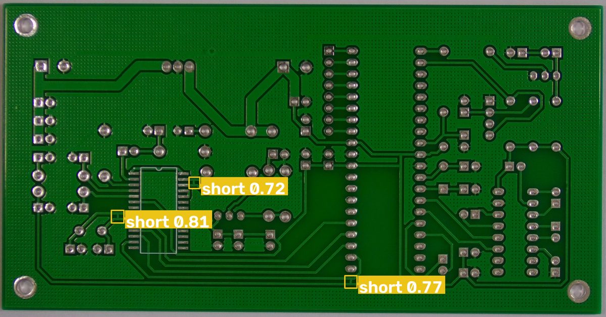
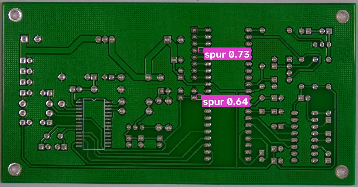
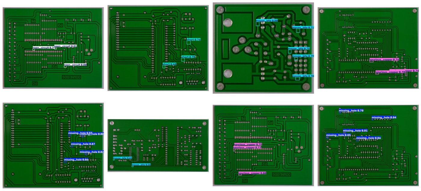
Targets the six defect categories most frequently encountered in PCB manufacturing and quality control. Detected locations are automatically marked with boxes, ready for manual review.
Component mounting hole absent, affecting insertion and soldering.
Irregular notch along the board edge, usually from mechanical damage.
Broken trace that interrupts signal conduction.
Unintended connection between adjacent traces, posing burn-out risk.
Excess copper spike along a trace edge, degrading electrical performance.
Stray copper residue on the board surface that needs removal.
WORKFLOW
No complex setup — as simple as taking a photo. Inspect right at the station.
Photograph the board with an industrial camera or smartphone, or import existing images from your archive.
→The system scans the entire board, identifies defects and computes their locations — finished in seconds.
→Defects are automatically boxed and listed. Inspectors simply review the marks against the board.
FIELD RESULTS
Actual outputs on real board photographs. Colored boxes mark defect locations automatically, with type labels attached.
PERFORMANCE
PCB manufacturers and QC teams are welcome to contact us — send sample boards and experience the detection results for free.